| Aaron's Homepage Forum |
| Home | Profile | Register | Active Topics | Members | Search | FAQ |
|
Note: You must be registered in order to post a reply.
|
|
|||||||||||
|
| This page was generated in 0.06 seconds. | Snitz Forums 2000 |
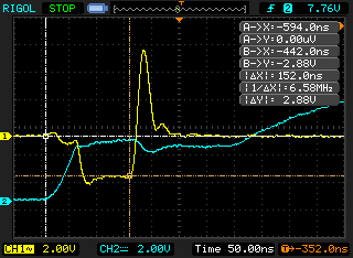 fr304_trr.png
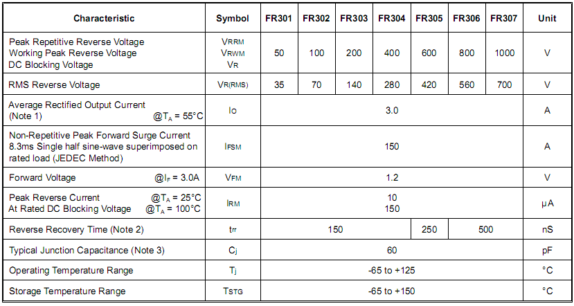 FR304_DSheet.png
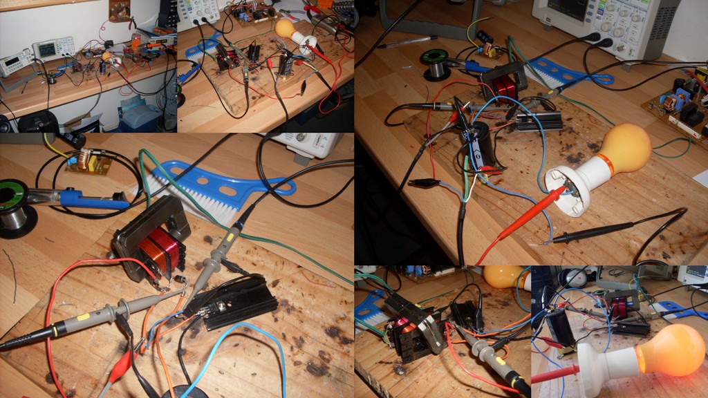 BoostSMPS_resize.jpg