| Author |
 Topic Topic  |
|
snarf
Apprentece

Malta
26 Posts |
 Posted - Oct 08 2014 : 3:38:59 PM Posted - Oct 08 2014 : 3:38:59 PM


|
quote:
Your Fig 1 is correct �my Fig 2 is wrong. Sorry about that. I must try to remember, �More haste � less speed�
That�s OK no problem, resolving difficulties helps me to learn. I always try hard to find the solution on my own first and ask only when I end with my back against the wall or when I�m not so sure with my conclusions .
quote:
It can be done, but my original circuit will need some changes, so I have now amended it. Here are the changes:
C5��������
Thank you so much for the new circuit and your in depth and detailed explanations which help me to understand and learn at the same time. Assembled on breadboard and tried out. Works to perfection and without problems, again many thanks.
The circuit is now more versatile, flexible and standalone, this makes it possible to use in other applications if required.
quote:
quote:
________________________________________
��� Can we take the output from Q14 of IC2 and feed it to pin 11 of IC1 maybe with a diode to drive IC1 pin 11 high, and modify the IC�s counter resetting to reset only IC2?
If��������
________________________________________
Although I was a bit off track I think that in a way my reasoning was in the right direction. Credit is all due to your kind and detailed explanations. From your circuit I can now see what I didn�t take into consideration and where I went wrong.
quote:
quote:
________________________________________
We had D1 removed from the circuit because it was not needed. For the sake of learning did D1 have any particular function or just not required?
________________________________________
In my first circuit it was put in to stop IC1. On reflection I thought it would not be needed because IC1 Q14 only stayed high for 10secs before IC2 output reset both counters via R3�����
I understood that D1 was to stop IC1 from counting further as you had already explained that before I posted my 4060 5sec + 5sec circuit, but since both IC�s are being reset when IC2 � Q14 goes high, stopping IC1 does not make much difference in that particular circuit (bearing in mind that the relay is switching OFF the timer�s circuit power). So I thought that is why D1 can be removed, or maybe D1 has a dual function that I�m not understanding. Therefore I decided to ask to have things clear in my mind. Thanks for the explanation.
quote:
quote:
________________________________________
Therefore it�s best to use �poly� capacitors and not �ceramic� capacitors because �ceramic� capacitors have a higher internal resistance?
________________________________________
No, it�s a question of stability at varying temperatures. Small ceramics up to about 100pF are very stable, but when you get up to 100nF you have to use a �High K� or a multiplayer ceramic. Neither of these is as stable as a polyester or a polystyrene cap. Although that doesn�t matter for decoupling caps it does matter if you are using them as timing caps. So when it comes to stocking caps for multi purposes, it pays to stock �polys� rather than ceramics, and where I get my supplies from they are cheaper.
I have been reading;
http://www.edn.com/design/analog/4416466/Signal-distortion-from-high-K-ceramic-capacitors
and
http://www.edn.com/design/analog/4426318/More-about-understanding-the-distortion-mechanism-of-high-K-MLCCs
Therefore if I understand properly a �High K� or multilayer ceramic will manifest a capacitance change with a voltage or temperature change?
Download Attachment:  Image 3.JPG Image 3.JPG
17.92�KB
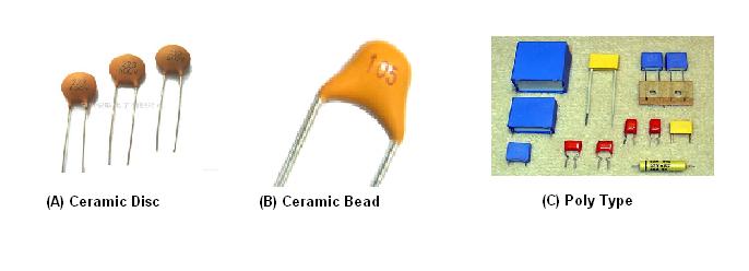
Do the images refer to the correct type of capacitors?
So image �B� is the �High K� multilayer ceramic, right?
So when using non polarized capacitors for timing it�s better to use poly capacitors, right?
Therefore from your explanation I would understand that it�s better to use �polys� also for other applications, I am always in difficulty when it comes to non polarized capacitors, is there a simple guide line?
The �polys� are slightly cheaper here as well.
Therefore using your last circuit as an example C2 and C3 would preferable be poly capacitors and C1 and C5 can be either ceramic or poly capacitors, is that right?
This question refers to C4 in your last circuit but is only intended for my learning.
When the circuit is switched OFF with C4 (100�F 25V) the charge in C4 takes a considerable time (about 15 to 20 seconds) to discharge to about 4V. If C4 is replace by a lower capacitance value, lets say 10�F 25V obviously the discharge time is much lower (about 5 seconds).
How can the charge in a capacitor be discharged quickly and safely without interfering with the capacitor�s function in the circuit? Do we add a resistor in parallel with the capacitor? If yes how do we calculate the value of the resistor?
|
Edited by - snarf on Oct 08 2014 3:46:13 PM |
 |
|
|
pebe
Nobel Prize Winner

United Kingdom
1078 Posts |
Posted - Oct 10 2014 : 09:07:24 AM
|
quote:
Therefore if I understand properly a �High K� or multilayer ceramic will manifest a capacitance change with a voltage or temperature change?
Do the images refer to the correct type of capacitors?
So image �B� is the �High K� multilayer ceramic, right?
So when using non polarized capacitors for timing it�s better to use poly capacitors, right?The �polys� are slightly cheaper here as well.
Therefore using your last circuit as an example C2 and C3 would preferable be poly capacitors and C1 and C5 can be either ceramic or poly capacitors, is that right?
Your assumptions are all correct.
quote:
Therefore from your explanation I would understand that it�s better to use �polys� also for other applications, I am always in difficulty when it comes to non polarized capacitors, is there a simple guide line?
I only use ceramics for the smaller capacities for RF work.
For coupling or decoupling where stability is not important then the larger ceramics would be OK, but their temperature coefficient is too large to use them for timing purposes. They are also usually more expensive than polys so for all these purposes I use polyester or polycarbonate types exclusively.
quote:
When the circuit is switched OFF with C4 (100�F 25V) the charge in C4 takes a considerable time (about 15 to 20 seconds) to discharge to about 4V. If C4 is replace by a lower capacitance value, lets say 10�F 25V obviously the discharge time is much lower (about 5 seconds).
How can the charge in a capacitor be discharged quickly and safely without interfering with the capacitor�s function in the circuit? Do we add a resistor in parallel with the capacitor? If yes how do we calculate the value of the resistor?
Yes, you can add a resistor in parallel with the capacitor. It discharges the cap quickly at first because there is max volts across the resistor. As the voltage drops, the current through the resistor also drops and the cap discharges at a slower rate. So the resulting discharge curve is an exponential one.
You can calculate the voltage across the capacitor quite easily.
The �Time Constant� of a resistor/capacitor combination (either in series or in parallel) is the product of capacity (in Farads) and resistance (in Ohms). You get the same result with the easier-to-use combination of microfarads and megohms. Now to calculate:
Remaining voltage across cap (as a proportion) = natural log to the power of minus (time / time constant.)
So remaining V = e^ -(T/TC)
If you use 10�F and 100K, the TC = 1sec, so the proportion of initial voltage remaining will be:
After 1.0sec e^ -1.0 = .368
After 1.5sec e^ -1.5 = .223
After 2.0sec e^ -2.0 = .135
After 2.5sec e^ -2.5 = .082
After 3.0sec e^ -3.0 = .049
After 4.0sec e^ -4.0 = .018
After 5.0sec e^ -5.0 = .006
So from this you can work out that if you choose 10�F and 100K, then after 4secs the cap will have discharged down to 1.8% of its original voltage.
I hope that all makes sense.
|
Edited by - pebe on Oct 11 2014 07:57:35 AM |
|
|
|
snarf
Apprentece
Malta
26 Posts |
Posted - Oct 14 2014 : 1:31:55 PM
|
Thank you for your reply and sorry for my late response.
quote:
I only use ceramics for the smaller capacities for RF work.
For coupling or decoupling where stability is not important then the larger ceramics would be OK, but their temperature coefficient is too large to use them for timing purposes. They are also usually more expensive than polys so for all these purposes I use polyester or polycarbonate types exclusively.
OK understood.
I am aware that tantalum capacitors are more expensive and that common tantalum capacitance values available range from 0.047�F (47nF) to around 680�F, but since tantalum are also ideal for timing purposes how do tantalum compeer with polys?
quote:
Yes, you can add a resistor in parallel with the capacitor. It discharges the cap .......
Thanks for detailed explanation, helps me understand and learn how to calculate the capacitor discharge value after a time period. Most appreciated.
Download Attachment: Image 4.JPG
5.33 KB
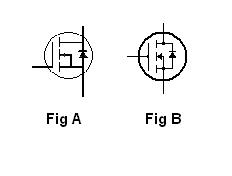
The file containing circuit symbols, which you kindly provided, contains two symbols that I am not familiar with, these are Fig A and Fig B. I have tried searching on the internet without finding an answer. Could you please indicate to which type of transistor these symbols refer to?
|
|
|
|
pebe
Nobel Prize Winner
United Kingdom
1078 Posts |
Posted - Oct 17 2014 : 12:14:19 PM
|
quote:
I am aware that tantalum capacitors are more expensive and that common tantalum capacitance values available range from 0.047�F (47nF) to around 680�F, but since tantalum are also ideal for timing purposes how do tantalum compeer with polys?
Both have good insulation and low equivalent series resistance so both can be used for timing circuit. But tantalum capacitors are normally polarised, which means they cannot be used as the timing component in any oscillator where polarity of the cap changes every half cycle � typically one made from gates as in the CD4060 you have just used. Polys there are a must. Tants can be used in other oscillators where polarity does not change, ie. in a 555 where the cap just charges and discharges, and when size is an important consideration.
They can also be used at either side of a voltage regulator, where typically 0.22�F is needed for filtering. The tant�s small size and low ESR score in its favour here. However they are not good for use in filtering power supplies where high ripple is present.
quote:
The file containing circuit symbols, which you kindly provided, contains two symbols that I am not familiar with, these are Fig A and Fig B. I have tried searching on the internet without finding an answer. Could you please indicate to which type of transistor these symbols refer to?
I didn�t realise both symbols were present. I made that file up by copying symbols used in other people's circuits and hadn�t realized I had duplicates. They are both the same and you can delete one of them.
They show an N channel IGFET with an inbuilt zener to provide clamping when driving inductive loads. If you look up the data sheet for an IRF530 it will tell you more about it.
For more information about electronics, you may find this website interesting. It contains some very useful information
http://www.electronics-tutorials.ws
|
|
|
|
snarf
Apprentece
Malta
26 Posts |
Posted - Oct 19 2014 : 5:40:50 PM
|
Thank you for your detailed reply.
quote:
Both have good insulation and low equivalent series resistance so both can be used for timing circuit. But tantalum capacitors are normally polarised, which means they cannot be used as the timing component in any oscillator where polarity of the cap changes every half cycle � typically one made from gates as in the CD4060 you have just used.
From your previous explanations I did understand that polarised capacitors such as tantalums can not be used with the CD4060 or similar, but thank you for pointing it out again. My question was for a comparison of the two different types of capacitors and your reply also explains it, thank you.
What I don�t understand is why some CD4060 circuits are using polarised capacitors like the circuit found here.
http://www.coolcircuit.com/circuit/timer_4060/
quote:
I didn�t realise both symbols were present. I made that file up by copying symbols used in other people's circuits and hadn�t realized I had duplicates. They are both the same and you can delete one of them.
They show an N channel IGFET with an inbuilt zener to provide clamping when driving inductive loads. If you look up the data sheet for an IRF530 it will tell you more about it.
Thank you for explaining. The IGFET is new for me. It was the diode symbol in both Fig A and Fig B, and the missing arrow which indicates the type of channel in Fig A that confused me, so I thought it�s better to ask.
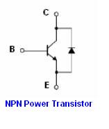
From your explanation I learned that some Power Transistors like the BUL381D also have a similar protection diode integrated, called the �antiparallel collector-emitter diode� , but this is a diode and not a Zener diode, is that right?
Download Attachment: NPN Power Transistor.JPG
4.12 KB
I have come across a collection of high quality symbols which may be useful. They can be downloaded from here.
http://www.circuitstune.com/2012/07/electrical-schematic-symbols.html
quote:
For more information about electronics, you may find this website interesting. It contains some very useful information
http://www.electronics-tutorials.ws
Many thanks for the link, very useful to me.
I have found a used and damaged 555 timer which has a broken relay and PCB. I could not test it but managed to draw a circuit.
Download Attachment: 555 CCT QST.JPG
37.4 KB
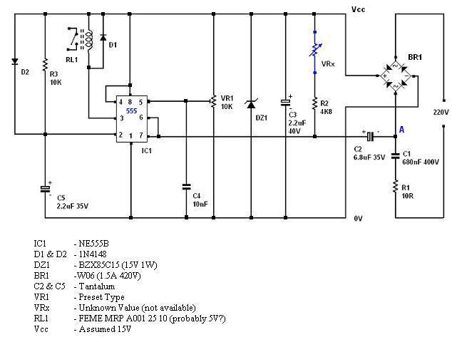
I am not understanding the circuit fully can you please help with some explanations?
1. From what I understand the timing RC are VRx + R2 and C2. Why is C2 connected to the AC source (marked A in diagram) instead of being connected to 0V (GND)? Is it using the mains 50Hz and why?
2. Capacitor C1 (680nF) should provide a continuous current of approximately 45mA, which I would assume is required to operate the circuit and the relay. When the relay is not energised the circuit will not require all that current but C1 still gives the same current, so where does the excess current go?
3. Why is the circuit using voltage control (VR1)? I assume Vcc to be +15V, why not use a lower Vcc instead of using voltage control (VR1), or is VR1 also dissipating the excess current?
4. Should D2 discharge C5 when power is switched off? If yes D2�s direction should be opposite, right?
General 555 question.
Download Attachment: 555 Load.JPG
10.67 KB
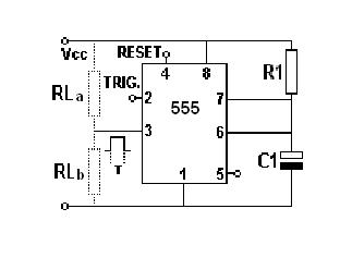
The output form a 555 IC can be taken from either pin 3 to Vcc rail (RLa), or pin 3 to GND rail (RLb).
Apart from the opposite output function of both options is it advisable to opt for (RLb) configuration or it does not make any difference?
Is it true that the 555 IC is more loaded with an (RLa) configuration and heats up more?
|
|
|
|
pebe
Nobel Prize Winner
United Kingdom
1078 Posts |
Posted - Oct 22 2014 : 02:22:12 AM
|
Re the 4060 circuit you gave a link to. I don�t know if the person who drew it up ever tested it, but it is very �iffey�. The cap has to charge up to half supply voltage, and polarity changes every half cycle. I think it highly unlikely that the electrolytic could reverse charge via 10K to that voltage � I think the reverse leakage current would be too high. But if it did, it would be impossible to calculate the oscillator frequency � there would be too many unknowns.
I don�t know about the BUL381D; I�ve never come across it. I see that is a high speed switching transistor used in switch mode supplies, so the diode may be there to suppress spikes when switching an inductive load. Perhaps someone else can give a more positive answer.
Thanks for the symbols � I�ll add them to my library.
The 555 circuit doesn�t make any sense to me, and I cannot see what it is supposed to do. Are you sure you have drawn it correctly?
D2 would take pin2 voltage up with the supply rail when the circuit was first switched on. That would serve no useful purpose because pin2 is the trigger pin and it needs to go below 1/3 supply voltage to trigger the 555. I think you are right and the diode has been fitted in reverse in error.
The 15V supply is obtained by using the energy in C1 each half cycle to �pump up� C3. As soon as C3 reaches 15V, DZ1 will start to conduct to keep Vcc constant. Accordingly, when the relay energises and takes current, less current will go through DZ1.
Now for the rest of the circuit. Assume D2 to be correctly fitted. At switch-on C3 would be low and would trigger the 555. Pin3 would go high, keeping the relay off. Then C3 would charge up via R3 to 15V and would have no further effect on the circuit.
If the RH side of C2 were connected to 0V instead of point �A�, then C2 would charge and pin6 would rise to 2/3 of Vcc. At that point pin3 would go low turning on the relay and pin7 would go low discharging C2. There the operation would end, so I think the circuit is intended to delay operation of the relay for some fixed time each time the unit was switched on.
Point �A� goes from �0.7V to +15.7V during a mains cycle. C2 would pass that change on to pin6 and the 555 would reset. Pin7 would switch to 0V and so an AC voltage would appear across C2, with an unknown result. So I think the C2 connection to �A� is in error.
About VR1: Inside the 555 are 3 equal value resistors in series. Their two junctions provide the two reference points of 1/3Vcc and 2/3Vcc for triggering pins2 & 6. The 2/3Vcc is taken out to pin5, so varying the voltage on that pin will affect the timing. I think VRx is probably a user adjustable pot to alter the delay period, and VR1 would be factory preset to allow for the tolerances of C2, R2 and VRx.
quote:
General 555 question.
The output form a 555 IC can be taken from either pin 3 to Vcc rail (RLa), or pin 3 to GND rail (RLb).
Apart from the opposite output function of both options is it advisable to opt for (RLb) configuration or it does not make any difference?
Is it true that the 555 IC is more loaded with an (RLa) configuration and heats up more?
The �standard� LM555 uses bipolar transistors. Pin3 is switched to 0v (output current is �sunk�) by an NPN transistor that switches down to within about 50mV of the 0V rail. But pin3 is lifted to Vcc (current is sourced) by two transistors in a Darlington arrangement configured as an emitter follower. There is an inherent voltage drop of at least two diodes in series, plus some extra depending on load. So with Vcc equal to 15V, pin3 would go no higher than 12.5V to 13.3V.
So there is 2V less available when using RLb rather than RLa. That has to be allowed for when deciding the voltage of the relay coil to use.
So RLb in less efficient than RLa, and there is an extra power of [2V x Load current] dissipated as heat in the 555.
The CMOS version, LCM555 has a lower maximum output current. It uses FETs for the output switches and they switch almost to 0V and Vcc, so RLa or RLb will both deliver the same voltage to the load.
|
|
|
|
snarf
Apprentece
Malta
26 Posts |
Posted - Oct 30 2014 : 5:15:14 PM
|
quote:
Re the 4060 circuit you gave a link to. I don�t know if the person who drew it up ever tested it, but it is very �iffey�. The cap has to charge up to half supply voltage, and polarity changes every half cycle. I think it highly unlikely that the electrolytic could reverse charge via 10K to that voltage � I think the reverse leakage current would be too high. But if it did, it would be impossible to calculate the oscillator frequency � there would be too many unknowns.
That is only one example out of many others. Unfortunately for those like myself who are trying to learn end confused as circuits like these are misleading. I was lucky that you had kindly explained the difference a while back and this made me realise the ambiguity in the circuit.
quote:
The 555 circuit doesn�t make any sense to me, and I cannot see what it is supposed to do. Are you sure you have drawn it correctly?
I have checked the circuit a couple of times and the drawn circuit I posted seems to be correct. An important point I forgot to mention is that some of the soldering on the PCB looks different from the rest of the soldering. This gives me the impression that it might have undergone some kind of repair and that might explain the wrong orientation of D2 and the connection of C2 to point �A�.
quote:
D2 would take pin2 voltage up with the supply rail when the circuit was first switched on. That would serve no useful purpose because pin2 is the trigger pin and it needs to go below 1/3 supply voltage to trigger the 555. I think you are right and the diode has been fitted in reverse in error.
The 15V supply is obtained by using the energy in C1 each half cycle to �pump up� C3. As soon as C3 reaches 15V, DZ1 will start to conduct to keep Vcc constant. Accordingly, when the relay energises and takes current, less current will go through DZ1.
Now for the rest of the circuit. Assume D2 to be correctly fitted. At switch-on C3 would be low and would trigger the 555. Pin3 would go high, keeping the relay off. Then C3 would charge up via R3 to 15V and would have no further effect on the circuit.
If the RH side of C2 were connected to 0V instead of point �A�, then C2 would charge and pin6 would rise to 2/3 of Vcc. At that point pin3 would go low turning on the relay and pin7 would go low discharging C2. There the operation would end, so I think the circuit is intended to delay operation of the relay for some fixed time each time the unit was switched on.
Point �A� goes from �0.7V to +15.7V during a mains cycle. C2 would pass that change on to pin6 and the 555 would reset. Pin7 would switch to 0V and so an AC voltage would appear across C2, with an unknown result. So I think the C2 connection to �A� is in error.
About VR1: Inside the 555 are 3 equal value resistors in series. Their two junctions provide the two reference points of 1/3Vcc and 2/3Vcc for triggering pins2 & 6. The 2/3Vcc is taken out to pin5, so varying the voltage on that pin will affect the timing. I think VRx is probably a user adjustable pot to alter the delay period, and VR1 would be factory preset to allow for the tolerances of C2, R2 and VRx.
Many thanks for your detailed explanations to my questions and circuit function, it makes more sense now.
quote:
The �standard� LM555 uses bipolar transistors. Pin3 is switched to 0v (output current is �sunk�) by an NPN transistor that switches down to within about 50mV of the 0V rail. But pin3 is lifted to Vcc (current is sourced) by two transistors in a Darlington arrangement configured as an emitter follower. There is an inherent voltage drop of at least two diodes in series, plus some extra depending on load. So with Vcc equal to 15V, pin3 would go no higher than 12.5V to 13.3V.
So there is 2V less available when using RLb rather than RLa. That has to be allowed for when deciding the voltage of the relay coil to use.
So RLb in less efficient than RLa, and there is an extra power of [2V x Load current] dissipated as heat in the 555.
The CMOS version, LCM555 has a lower maximum output current. It uses FETs for the output switches and they switch almost to 0V and Vcc, so RLa or RLb will both deliver the same voltage to the load.
OK I understand the difference between output options RLa and RLb and yes very important to always keep account of the load current.
Have read the LCM555 datasheet and although the output load current is 100mA maximum instead of the 200mA output load current for the LM555 specifications indicate that the LCM555 is more stable and accurate, lower power dissipation and oscillator frequency up to 3MHz in astable mode.
I have greatly appreciated the assistance and support given. With your (Edited : your not our) help I have managed to learn something. Many thanks to everyone in particular to Pebe who has been very patient with me and led me by the hand with his kind and detailed step by step explenations.
|
Edited by - snarf on Nov 11 2014 12:34:42 PM |
|
|
|
pebe
Nobel Prize Winner
United Kingdom
1078 Posts |
Posted - Nov 08 2014 : 11:02:25 AM
|
| I am pleased to have been of assistance, and if there is any other way I can help please come back. |
|
|
|
Topic |
|
|
|